|
|
Basic Semiconductor Physics
Introduction

|
Materials can be categorised into
conductors
,
semiconductors
or
insulators
by their ability to conduct electricity.
It is a popular belief that insulators do not conduct electricity because their valence electrons are not free to wander throughout the material. In fact they are free to move around, however, in an insulator there are as many electrons as there are energy levels for them to occupy. If an electron swaps place with another electron no change is made since electrons are indistinguishable. There are higher energy levels, but to promote the electrons to these energy levels requires more energy than is usually practical. |
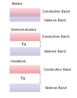
Metals conduct electricity easily because the energy levels between the conduction and valence band are closely spaced, or there are more energy levels available than there are electrons to fill them so very little energy is required to find new energies for electrons to occupy. The resistivity of a material is a measure of how difficult it is for a current to flow. Semiconductors have a resistivity between 10-4< ρ<108 Ω m although these are rough limits. The band theory of materials explains qualitatively the difference between these types of materials. Electrons occupy energy levels from the lowest energies upwards. However, some energy levels are forbidden because of the wave like properties of atoms in the material. The allowed energy levels tend to form bands. The highest filled level at T=0 K is known as the valence band . Electrons in the valence band do not participate in the conduction process. The first unfilled level above the valence band is known as the conduction band . In metals, there is no forbidden gap; the conduction band and the valence band overlap, allowing free electrons to participate in the conduction process. Insulators have an energy gap that is far greater than the thermal energy of the electron, while semiconductor materials the energy gap is typically around 1eV. The diagram below shows the differences in metals, semiconductors and insulators in terms of the how the energy bands are separated
Elemental semiconductors are semiconductors where each atom is of the same type such as Ge, Si. These atoms are bound together by covalent bonds, so that each atom shares an electron with its nearest neighbour, forming strong bonds. Compound semiconductors are made of two or more elements. Common examples are GaAs or InP. These compound semiconductors belong to the III-V semiconductors so called because first and second elements can be found in group III and group V of the periodic table respectively. In compound semiconductors, the difference in electro-negativity leads to a combination of covalent and ionic bonding. Ternary semiconductors are formed by the addition of a small quantity of a third element to the mixture, for example Al x Ga 1-x As. The subscript x refers to the alloy content of the material, what proportion of the material is added and what proportion is replaced by the alloy material. The addition of alloys to semiconductors can be extended to include quaternary materials such as Ga x In (1-x) As y P (1-y) or GaInNAs and even quinternary materials such as GaInNAsSb. Once again, the subscripts denote the proportion elements that constitute the mixture of elements. Alloying semiconductors in this way allows the energy gap and lattice spacing of the crystal to be chosen to suit the application.
Intrinsic semiconductors are essentially pure semiconductor material. The semiconductor material structure should contain no impurity atoms. Elemental and compound semiconductors can be intrinsic semiconductors. At room temperature, the thermal energy of the atoms may allow a small number of the electrons to participate in the conduction process. Unlike metals, where the resistance of the material decreases with temperature. For semiconductors, as the temperature increases, the thermal energy of the valence electrons increases, allowing more of them to breach the energy gap into the conduction band. When an electron gains enough energy to escape the electrostatic attraction of its parent atom, it leaves behind a vacancy which may be filled be another electron. The vacancy produced can be thought of as a second carrier of positive charge. It is known as a hole . As electrons flow through the semiconductor, holes flow in the opposite direction. If there are n free electrons in an intrinsic semiconductor, then there must also be n holes. Holes and electrons created in this way are known as intrinsic charge carriers. The carrier concentration, or charge density, defines the number of charge carriers per unit volume. This relationship can be expressed as n=p where n is the number of electrons and p the number of holes per unit volume. The variation in the energy gap between different semiconductor materials means that the intrinsic carrier concentration at a given temperature also varies.

An extrinsic semiconductor can be formed from an intrinsic semiconductor by adding impurity atoms to the crystal in a process known as doping . To take the most simple example, consider Silicon. Since Silicon belongs to group IV of the periodic table, it has four valence electrons. In the crystal form, each atom shares an electron with a neighbouring atom. In this state it is an intrinsic semiconductor. B, Al, In, Ga all have three electrons in the valence band. When a small proportion of these atoms, (less than 1 in 10 6 ), is incorporated into the crystal the dopant atom has an insufficient number of bonds to share bonds with the surrounding Silicon atoms. One of the Silicon atoms has a vacancy for an electron. It creates a hole that contributes to the conduction process at all temperatures. Dopants that create holes in this manner are known as acceptors. This type of extrinsic semiconductor is known as p-type as it creates positive charge carriers. Elements that belong to group V of the periodic table such as As, P, Sb have an extra electron in the valence band. When added as a dopant to intrinsic Silicon, the dopant atom contributes an additional electron to the crystal. Dopants that add electrons to the crystal are known as donors and the semiconductor material is said to be n-type.
Doping of compound semiconductors is slightly more complicated. The effect of the dopant atom depends on the site occupied by the atom in the lattice . In III-V semiconductors, atoms from group II act as a acceptors when occupying the site of a group III atom, while atoms in group VI act as donors when they replace atoms from group V. Dopant atoms from group IV have the property that they can act as acceptors or donors depending on whether they occupy the site of group III or group V atoms respectively. Such impurities are known as amphoteric impurities
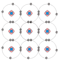
Intrinsic |
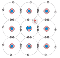
p-type |
n-type |
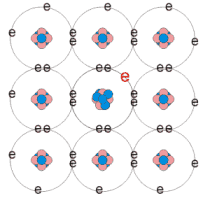
Schematic diagram showing the only the valence electron shell to illustrate intrinsic, p-type and n-type semiconductors.
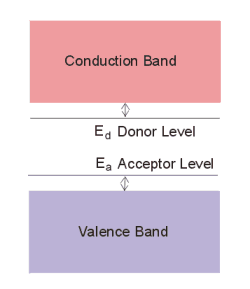
Often, we are interested in transitions that occur near the bottom of the conduction band minimum to valence band maximum; In this case, it is useful to draw the bandstructure energy as a function of position, setting the wavevector k =0. In this representation of the energy bands, the donors and acceptors form levels in the energy gap region. At T=0 K, any free carriers from donors and acceptors are bound to their atoms. So there is no conduction. For non-zero temperatures, the sites can be thermally ionised, releasing carriers in the bands so conduction can occur.
|
|
|
These shallow level impurities are known as hydrogenic impurities . For donor atoms, an electron orbits a lattice site, while for acceptors a hole orbits around a lattice site with residual negative charge. The energy required to ionise these carrier is much less than the binding energy of the hydrogen atom since the effective mass is smaller and the radius of the carrier orbit larger than that of the hydrogen atom. A table of common impurities and their activation energy is to be found in the reference section.
![]()
A rough estimate for the temperature of ionisation is
![]() at room temperature. Initially when the temperature is low, excitation from
donors and acceptors can be the only source of carriers: in this range the
conductivity is extrinsic. In this regime, the doping of the semiconductor
determines whether the semiconductor is n-type or p-type. At higher enough
temperatures, direct thermal excitation from the valence band to the conduction
band swaps the extrinsic density. There is then an equal number of electrons
and holes; the conductivity is intrinsic with distinction between n and p.
at room temperature. Initially when the temperature is low, excitation from
donors and acceptors can be the only source of carriers: in this range the
conductivity is extrinsic. In this regime, the doping of the semiconductor
determines whether the semiconductor is n-type or p-type. At higher enough
temperatures, direct thermal excitation from the valence band to the conduction
band swaps the extrinsic density. There is then an equal number of electrons
and holes; the conductivity is intrinsic with distinction between n and p.
Band Structure and Effective Mass
The basic description of a semiconductor is its bandstructure, i.e. the variation of energy E with wave-vector k . The most important bands are:
Valence band - the last filled energy level at T=0 K
Conduction band - the First unfilled energy level at T=0 K
The valence band maximum is at k =0, is known as the gamma point . Where the conduction-band minimum also occurs at k =0, the semiconductor is said to be a direct band semiconductor. At non-zero k =0, the semiconductor is an indirect-band semiconductor . In addition to these two main conduction bands, other bands may also be present. In III-V semiconductors, Ge and Si there are 3 valence bands with maxima at k =0. These are the light-hole , heavy-hole and spin-orbit split-off band .
The bands in a semiconductor material are approximated by parabolic functions of k close to the bandedges.

Conduction-band:
![]()
Valence-band:
![]()
The expression for the effective mass is found from the dynamics of a wave-packet, which represents a localised particle. The wave packet is a modulation envelope, with a carrier-wave running through it. The packet is made up of a small spread of frequencies w around a central value w 0 ; these are superimposed on each other. The wave packet moves at the group velocity v g
![]()
If an electric field E f is applied, so that the wave packet moves a distance dx in time dt. The change in energy of the wave packet is
![]()
This change corresponds to a change dk of the central k value k 0 ; it is given by
![]()
We convert this to a time derivative:
![]()
But
![]() , so
, so
![]()
The equation for the acceleration, can be calculated from
![]()
![]()
![]()
Substituting for
![]() from our first major result,
from our first major result,
![]()
![]()
Comparing these forms, we see,
![]()
The dynamics of the holes is more complicated. It is necessary to consider one unfilled state in the otherwise filled valence band. The result is that the hole mass acts like a particle with positive charge + e and mass m h given by
![]()
The Fermi Level and Intrinsic Semiconductors
Electrons are Fermions , and thus follow Fermi-Dirac distribution function
![]()
where μ is the Fermi Energy often denoted E f or chemical potential, in semiconductor physics, is the energy at which there would be a fifty percent chance of finding an electron, if all energy levels were allowed. In order to apply the statistics, we need the density of states in the conduction and valence bands. These are derived from the basic principle that the density of states is constant in k-space. In the conduction band the density of states is given by:
![]()
and the valence band,
![]()
where E is measured from the top of the valence band.

![]()
The density of electrons in the conduction band is
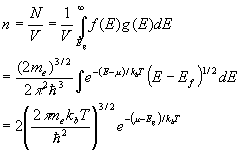
(18)
In the valence band, the probability of a hole is
![]()
and can be approximated
![]()
A similar calculation yields the hole density

(21)
Calculation of the Fermi level given the carrier concentration is useful in the calculation of laser gain, but since the function is not invertable, there is no analytical method for achieving this. However numerous approximations have been forumulated to calculate the Fermi level.
The value of μ depends on N a and N d . However μ can be eliminated between (18) and (21) to give the important relation
![]()
(22)
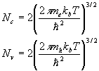
where N c and N v are the prefactors in (18) and (21) .
As stated, (22) holds for all T and independent of the values of N a and N d . In the intrinsic region, the extrinsic density is negligible, and then n=p since each electron excited to the conduction band leaves a hole behind it. In the intrinsic region, therefore
![]()
(24)
If we substitute into (24) the values of n and p from (18) and (21)
![]()
This gives the value of μ in the intrinsic region, simple manipulation leads to

That is, μ is displaced from the middle of the band gap by a temperature dependent term that depends on the ratio of the effective masses.
The Fermi Level and Extrinsic Semiconductors
What happens to μ with temperature when donors and acceptors are present? The charge neutrality condition governs the numbers of carriers.
![]()
(27)
where N a - and N d + are the number of ionised acceptor and donor sites. The number of sites that are ionised is:
![]()
(28)
A similar argument shows that
![]()
(29)
The four terms in (27) are given in terms of μ (18) , (29) , (21) and (28) respectively, so μ can in fact be determined from (19). The general case has to be dealt with numerically;
We take the case of n-type doping but with some counter-doping:
![]() and
and
![]()
(30)
at T=0, N a electrons move off donor sites to occupy the acceptor sites. Thus
![]()
(31)
The donor sites are partially occupied. This is only possible at T=0 if the Fermi-level is at the donor-site energy:
![]()
(32)
This will not change for very low temperatures,
![]() , so substitution of the value of μ into
(18)
gives
, so substitution of the value of μ into
(18)
gives
![]() for
for
![]()
(33)
It is seen that (29) is definitely a low-temperature result. For p-type doping, the result corresponding to (33) is
![]() for
for
![]()
(34)
The important technical region in the n-type material is the temperature range in which all the donors are ionised and the extrinsic electron density is higher than the intrinsic density. Full ionisation means:
![]()
(35)
Since N a electrons are required for occupation of the acceptor sites. Comparison of (24) and (7) gives

(36)
The corresponding results for p-type doping are
![]()
(37)

(38)
Note that in this technical region if the counter doping is negligible,
![]() or
or
![]() ,
(35)
and
(37)
simplify to
,
(35)
and
(37)
simplify to
![]()
![]()
(40)
which is what we tell the engineers.
|
|
