|
|
The p-n Junction

Junctions are crucial to many semiconductor applications. The oldest method of making a p-n junction is by diffusion. The dopant diffuses in under heating so that the surface acceptor concentration exceeds the donor concentration. A junction appears when N d =N a
Another doping technique is ion implantation. The starting material, n-type only, is bombarded with the required species of ions, say acceptors. This produces sharper junctions, but causes damage to the crystal lattice structure increasing the number of dislocations and interstitial atoms.
Epitaxial deposition techniques are now widely established. The starting material is a single crystal in all cases, so it is possible to grow further crystal layers which are in register with the starting crystal. The most precise although most expensive way of achieving this is Molecular Beam Epitaxy (MBE). Ions of the semiconductor together with dopants are fired at the crystal surface. Under the right conditions (ultrahigh vacuum, correct ion fluxes, correct substrate temperature) the crystal grow epitaxially with the required dopant included. This technique can produce very sharp junctions and there is no counter-doping, i.e. no donors in the p-type region. Discussion on fabrication from crystal growth to etching, other expitaxial growth methods, up to metalisation and etching is outlined here . We are supposed to be discussing p-n junctions!
We now consider a p-n junction in the absence of voltage
bias, so that it is in thermodynamic equilibrium. This means that the
chemical potential
![]() must
be constant across the junction. Since
must
be constant across the junction. Since
![]() is near the valence band edge in a p-type region and near the
conduction
band in an n-type region, the bands must bend through the junction as
shown below:
is near the valence band edge in a p-type region and near the
conduction
band in an n-type region, the bands must bend through the junction as
shown below:
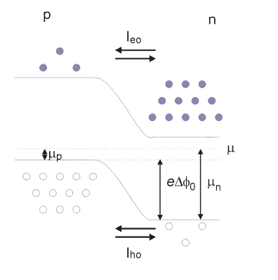
In the region where the bands are bending,
![]() is near the middle of the gap and therefore n<n
0
, p<p
0
,
where n
0
and p
0
are the concentrations deep inside
the n and p type regions. This is therefore called the depletion
region.
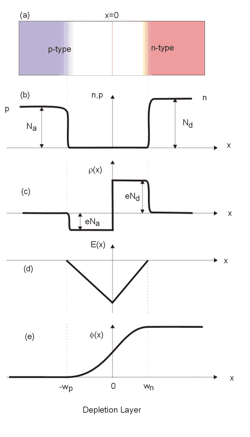
If we assume the junction is sharp, with N
a
and N
d
changing abruptly at the junction, and assume N
d
=N
a
,
p
0
=N
a
, thus we see that within the depletion region
p<N
A
on the left and n<N
d
on the right. Since
N
A
and N
D
are the densities of ionised acceptor
and donor ions, this means that there is a net negative charge on the
p-type side of the junction, and a net positive charge on the n-type
side.
These separated charges generate an electric field, which is the
physical
cause of the band bending. The overall picture is summarised below.
is near the middle of the gap and therefore n<n
0
, p<p
0
,
where n
0
and p
0
are the concentrations deep inside
the n and p type regions. This is therefore called the depletion
region.
If we assume the junction is sharp, with N
a
and N
d
changing abruptly at the junction, and assume N
d
=N
a
,
p
0
=N
a
, thus we see that within the depletion region
p<N
A
on the left and n<N
d
on the right. Since
N
A
and N
D
are the densities of ionised acceptor
and donor ions, this means that there is a net negative charge on the
p-type side of the junction, and a net positive charge on the n-type
side.
These separated charges generate an electric field, which is the
physical
cause of the band bending. The overall picture is summarised below.

We now calculate charge, electric field and potential. First we find
the band offset.
![]() ,
i.e. the difference in the height of
,
i.e. the difference in the height of
![]() above the valence band on the two sides. In the n-type region, the
value
of
above the valence band on the two sides. In the n-type region, the
value
of
![]() relative
to the local valence band is given by
relative
to the local valence band is given by
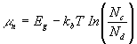
(1)
assuming N A =0 on the n-side. On the p-type side, we have

(2)
assuming N D =0 on this side. These give
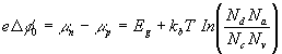
(3)
Using the definition of the intrinsic density n i (24, semiconductor basics) , gives
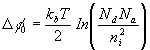
(4)
This is the difference in the electrostatic potential between the two sides
since
![]() is the energy difference between electrons at the bottom of the conduction
band on the two sides, as may be seen from the diagram.
is the energy difference between electrons at the bottom of the conduction
band on the two sides, as may be seen from the diagram.
The variation of
![]() and the electric field
and the electric field
![]()
(5)
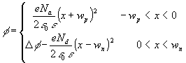
across the junction can be calculated as long as the variations with x of N D and N A are known. If we assume an abrupt junction then the charge distribution has the form:
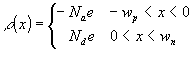
(6)
where w p and w n are the semi-widths of the depletion region on the p-side and n-side; values for them will be found later.
The electric field satisfies Gauss' law:
![]()
(7)
since
![]() with
with
![]() constant, and
in the present 1-d case
constant, and
in the present 1-d case
![]() ,
this gives
,
this gives
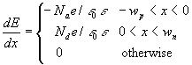
(8)
The boundary conditions are E=0 for x<-w p and x>w n since the junction is in equilibrium. The solution of (8) is therefore,
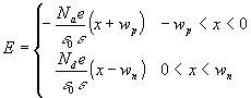 .
.
(9)
Furthermore, E must be continuous at x=0, which gives
![]()
(10)
As seen from the figure, this is simply the condition of electrical neutrality of the whole depletion region. The variation of E with x given is shown in (d)
Equations
(5)
and
(8)
together give
![]()
(11)
![]() must be continuous
at x=0; this gives a second relation between w
p
and w
n
:
must be continuous
at x=0; this gives a second relation between w
p
and w
n
:
![]()
(12)
Recall that
![]() is
already known from
(4)
. The variation of
is
already known from
(4)
. The variation of
![]() with x given by
(11)
and is shown in (c). As stated,
(4)
,
(11)
can
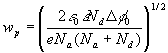
be solved for the values of w
p
and w
n
; they are,
with x given by
(11)
and is shown in (c). As stated,
(4)
,
(11)
can
be solved for the values of w
p
and w
n
; they are,
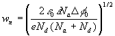
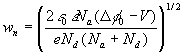
(13)
(14)
The dependence on T and on the doping deserves comment. Assuming for
simplicity N
A
=N
D
(equal doping on both sides), so
that the factors
![]() and
and
![]() are both one,
substitution of
(12)
for
are both one,
substitution of
(12)
for
![]() gives:
gives:
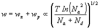
(15)
The logarithmic dependence is very weak compared with the denominator, so:
w increases as T increases
w decreases as doping N A +N D increases
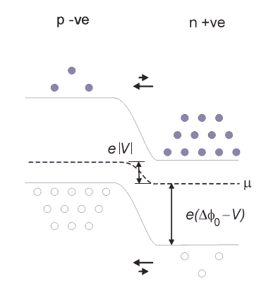
The application of p-n junctions depends on having an applied
voltage so that a current flows through the junction. With a voltage V
applied a difference eV appears between the values of
![]() on the p and n side. We distinguish between forward and reverse bias,
as in the diagram below:
on the p and n side. We distinguish between forward and reverse bias,
as in the diagram below:
Forward Bias
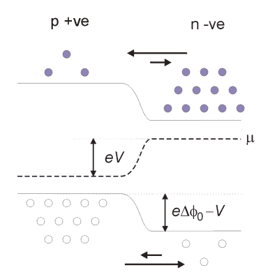
Reverse Bias
The calculation of
![]() etc. go through much as before, and give:
etc. go through much as before, and give:
(16)

(17)
There is a charge separation in the depletion region. Thus the depletion region behaves like a capacitor, and the capacitance is given by
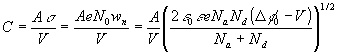
(18)
Where A is the area of the junction (in the y-z plane). This has the useful property that the capacitance can be varied by applied voltage. In practice, reverse bias is needed so that the current flow is small. A p-n junction device used as a voltage-variable capacitor is known as a varactor diode.
The important property of a p-n junction is the current-voltage characteristics. A derivation requires discussion of diffusion and recombination of carriers. The result is
![]()
(19)
where the predominant temperature dependence of I 0 is given by
![]()
(19)
The first semiconductor lasers where made from heavily doped p-n junctions. Under conditions of forward bias the electrons and holes would recombine at the barrier junction producing some laser emission at high currents. These devices were inefficient and had high threshold currents as the majority carriers tended to drift away from the junction interface. It was soon discovered that more efficient lasers could be produced by the implementation of a heterostructure design.
|
|