|
|
Single Crystal Growth
Liquid Encapsulated Czochralski Crystal Growth (LEC)
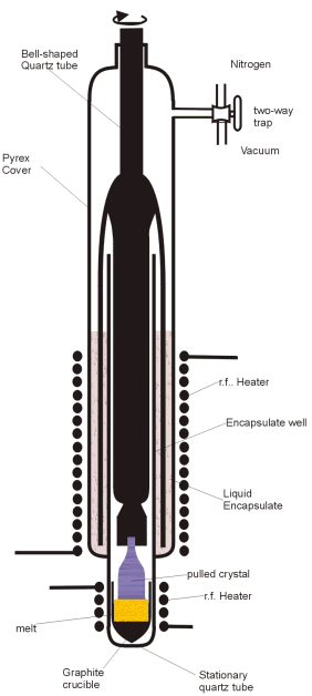
Figure 1. Liquid Encapsulated Czochrazski crystal pulling chamber |
The first step in making any device is to start with a wafer of semiconductor
material. These wafers are sliced from a large single crystal known as a
boule
. Figure 1 shows the apparatus used to grow the boule. A small seed crystal of
the material to be grown is lowered to the surface of the melt and then drawn
upwards, slowly. As the seed crystal is pulled from the melt, it draws with it
a layer of molten material. This material cools gradually, taking on the same
crystalline structure as the seed crystal. Pellets of dopant material are added
to the melt if extrinsic semiconductor material is required. Making compound
semiconductor crystals is somewhat more difficult because the vapour pressures
of the constituent materials are different. At the temperature required to melt
the higher temperature material, the lower melting-point material has
evaporated. Evaporation can prevented by the use of a liquid lid or
encapsulate. The encapsulate must of course be made of a material that is less
dense than the material in the crucible and must not be absorbed in the melt.
For making Indium Phosphide crystals, a Boric-Oxide (B
2
O
3
)
encapsulate, coupled with a high pressure of inert gas in the chamber, prevents
the volatile phosphorous from vaporising from the melt.
|

Wafer Preparation
The next stage of the fabrication process is to turn the single crystal of semiconductor material into many thinly sliced wafers. The boule of semiconductor has a non-uniform diameter. In commercial wafer processing, high yields depend on the uniformity of the wafers. The semiconductor crystal is machined on a lathe into a cylinder. The orientation of the crystal planes is fixed by the seed crystal, usually {100}, for many semiconductors including InP. The orientation within the plane must be fixed by x-ray diffraction. Once the geometry of the cylinder is established, a flat is ground along the its length. In devices such as Fabry-Perot lasers, the wafer has crucial cleavage planes that will form the mirrors. The cylinder is sliced into thin wafers using a diamond annular saw. The cut wafers have some saw marks that must be removed. This is achieved using a combination of mechanical polishing and chemical etching until the surface of the wafer is optically flat.
Expitaxial Growth Techniques
Molecular Beam Epitaxy (MBE)
A schematic diagram of an MBE machine is shown in Figure 3. Generally, these machines consists of three vacuum sections, of which the growth chamber is the most important. The buffer section is involved in the preparation and storage of the wafers before entering the growth chamber. While the load lock is used to insert and remove samples while retaining the integrity of the vacuum. Samples are loaded onto a rotational magnetic holder known by the acronym, Continual Azimuthal Rotation (CAR). Cyropanels are used in conjunction with the vacuum system to keep the partial pressure of undesirable gases such as CO 2 and H 2 O around 10 -11 Torr. The principle of operation is that gaseous substances are bound to the cold surfaces within the pump by means of cryocondensation, cryosorption or cryotrapping. Epitaxial growth starts with the many heated cells, called effusion cells or Knudsen cells, that contain a compound required for the addition of a particular atomic species into the vacuum chamber. Each sources is independently heated until atoms of the source material are able escape by thermionic emission. An advancement of MBE, Gas Source MBE (GSMBE), uses room temperature gases for the source materials, thus avoiding significant contamination problems and the necessary higher substrate temperatures that can cause segregation of dopant atoms.
Within the ultra-high vacuum, the free atoms have a long mean-free path and collisions with other atoms are infrequent. Atoms from the sources are able to travel in a straight line until they collide with the substrate material. A computer remotely operates the shutter controls, allowing the emission of different species of atom to be directed at the substrate. The typical rate of growth with MBE is around a single mono-layer per second. Although slow, this allows for abrupt changes in material composition. Under the right conditions, the beam of atoms will attach to the substrate material and an epitaxial layer will begin to form.
|
Figure 2. Schematic diagram of MBE machine. |
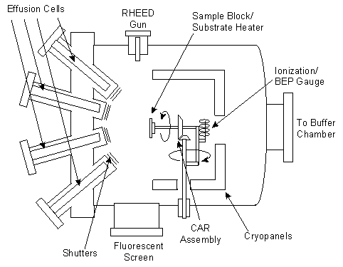
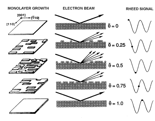
Control over the thickness is determined using an ion gauge mounted to face the beam sources. The Beam Equivalent Pressure (BEP) of the material sources can be used to measure the rate of growth of the layers. Alternatively, Reflection High-Energy Electron Diffraction (RHEED) is another useful measuring technique. Electrons are emitted from an electron gun at a glancing incidence to the CAR. The reflected and diffracted electrons emit light in a distinctive pattern when they strike a phosphor screen. Figure 3 shows the process simplified. Starting from a flat substrate, the electrons are not scattered greatly and are recorded as an intense beam. As material is deposited on the surface, the atoms create islands of epitaxial growth with a concomitant decrease the reflectivity of the surface of the material as the electrons are scattered. As the deposition process continues, material builds up on the surface, the islands join together and create new flat surfaces with the original substrate becoming voids in the newly created material. As yet more material forms, the voids begin to fill up and the reflectivity increases once again, although in reality, the reflectivity does not reach as high a value, since the process of deposition is random and the surface never regains the completely flat profile of the initial polished substrate. By monitoring the oscillations in the reflectivity one can estimate the thickness and rate of growth of the epitaxial material.
|
Figure 3. Reflection High-Energy Electron Deflection (RHEED) measurement system. Electrons are scattered more when a new mono-layer of atoms are being form. The intensity of the RHEED signal oscillates as new layers are progressively formed. |
Metal-Organic Chemical Vapour Deposition (MOCVD)
MOCVD or MOVPE (Metal-Organic Vapour Phase Epitaxy) is another widely used method of creating controllable epitaxial layered structures by atomic deposition over a substrate material.
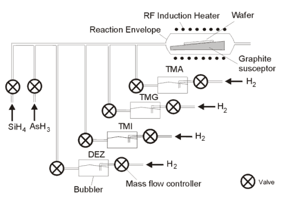
Figure 4 Schematic diagram of the MOCVD process. |
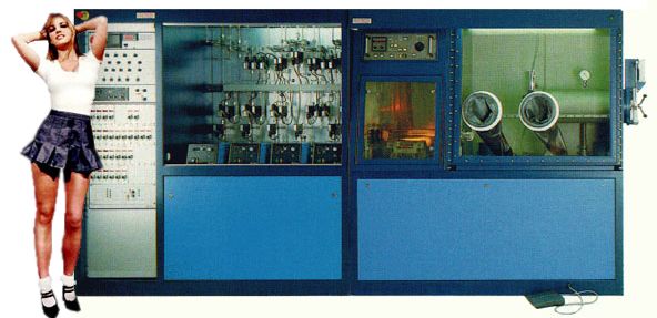
Figure 5 Britney and a real MOCVD machine. |
The substrate wafer is placed on a graphite susceptor inside a reaction vessel and heated by an RF induction heater. The temperature depends on the type of compounds grown, but it is usually between 500 ° C and 700 ° C. Growth occurs in an atmosphere of hydrogen at a pressure between 100 and 700 Torr. The growth precursors decompose on contact with the hot substrate to form epitaxial layers. Group V precursors are AsH 3 (arsine) while group III are Ga(CH 3 ) 3 Trimethylgallium (TMG). The other group III precursors shown in the diagram are: Al(CH 3 ) 3 Trimethylaluminium (TMA) for Aluminium, In(CH 3 ) 3 trimethylindium (TMI) for Indium, SiH 4 Silane for Silicon, AsH 3 Arsine for Arsenic and Zn(C 2 H 5 ) 2 Diethylzinc (DEZ) for Zinc.
Wafer Bonding
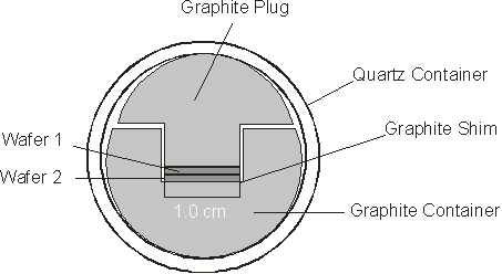
Figure 6. A schematic diagram of a wafer bonding vessel.
Wafer bonding is a method of fusing two semiconductor materials at the atomic level. This method is especially useful in bonding materials such as GaAs and InP which have different lattice constants. The technique has been used successful in creating long wavelength VCSELs with InGaAsP active regions and InP cladding layers bonded to GaAs/AlAs DBRs. ,, . The difference in refractive index of InP and GaInAsP, used is in epitaxial DBR mirrors is very small. At least 30-periods are required to achieve the desired reflectivity. GaAs/AlAs has a greater contrast in refractive index. Therefore fewer periods are required to achieve the same reflectivity but have slightly different lattice constants to InP. (Approx. 5.8Å for InP compared to approx. 5.6Å for GaAs/AlAs.) The wafers to be fused are placed within the quartz reactor. When heated the difference in the thermal expansion of the graphite and the quartz reactor cause the wafers to be compressed together. For successful fusion to occur, the wafers must be optically flat and free of contaminants. VCSELs created with the method showed normal device characteristics indicating the integrity of the fusion boundary. However, the effects of strain between the two kind of semiconductor at the boundary make the long-term reliability uncertain.
Mircofabrication
Lithography
Masks are created to define areas that will be protected or removed during the lithography stage. Photoresist is spin-coated onto the semiconductor wafer. A photoresist is a light-sensitive material that on exposure to ultra-violet light causes it to undergo a chemical reaction. This is similar to the action of light on a photographic film. The photoresist is developed creating a negative Image of the mask. An etchant will selectively etch away the material not protected by the photoresist. There are two types of photoresist that react in differently on exposure to ultra-violet light. If the photo-resist hardens on exposure to the light, when the excess resist is removed a negative copy of the mask is left behind and hence it is known as a negative photo-resist. Positive resists are designed to degrade on exposure to light. When developed, the resist is deposited in those areas where the light did not expose the resist, resulting in a positive copy of the mask.
For VCSELs, the typical dimensions of the contacts are suitable for ultra-violet light lithography to be used. The smaller features such as those found in integrated circuits require smaller wavelengths of light to be used. As more components are packed onto a single chip, this demands the use of techniques such as electron-beam lithography or x-ray lithography.
Metalisation
There are three techniques that are commonly used to create contacts: thin-film vacuum evaporation, sputtering and electroplating. With vacuum evaporation, the device is suspended above a Tungsten or Molybdenum boat containing the metal to be deposited on to the surface of the device. The boat is heated either by applying a current through it or by electron bombardment, vaporising the metal within the boat. Within the vacuum, atoms of the metal are emitted from the surface and travel in all directions, condensing on the inside of the bell-jar. A mask is used to control the geometry of the evaporated film on the device.
Sputtering also takes place within a bell-jar. The bell-jar is evacuated and an inert gas such as Argon is bled into the jar keeping a background pressure of 10 -2 Torr. The material to be deposited onto the surface acts as the cathode. When a high-voltage of 2-6kV is applied, the gas is ionised and the positive ions are accelerated to the cathode. The ions have sufficient energy to eject atoms of the cathode material. The mean free path of the atoms is long enough under the conditions of vacuum within the bell-jar to eventually coat the surface of the semiconductor.
Electroplating has the material to be plated acting as a cathode. Submerged in an aqueous solution of metal salts, a voltage applied across the cathode and anode causes the metal decomposes coating the substrate. Electroplating is more simple and cheaper than evaporation or sputtering. However, the resulting metallic coating is difficult to control in thickness, less pure than either evaporation or sputtering and with surface topography that relatively poor.
Etching
Etching may be required in the fabrication of VCSELs, for example to create the mesa structure of air post VCSELs or in creating areas for re-growth for current blocking layers. The most common method of etching material is chemical etching. Table 1 lists some chemical etchants, the materials they are designed to etch and the rate of etch.
|
Etchant and ratio of mixture
|
Material Etched
|
Approx. etch rate μ m per min at 20 ° C |
|
HCl (conc.) |
InP |
5-15 |
|
HCl (conc.) |
Surface oxide on GaAs |
Fast |
|
HCl (conc.) |
InGaAs |
<0.02 |
|
HCl:H 2 0 (2:1) |
InP |
8 |
|
HCl:H 2 O (1:1) |
InP |
0.7 |
|
HCl:H 2 O (1:2) |
InP |
0.09 |
|
H 3 PO 4 :HCl (1:1) |
InP |
2.5 |
|
H 3 PO 4 :HCl (1:2) |
InP |
4.8 |
|
H 3 PO 4 :HCl (1:3) |
InP |
6.6 |
|
H 3 PO 4 :HCl (3:1) |
InP |
0.75 |
|
H 3 PO 4 :H 2 O 2 :H2O (3:4:3) |
GaAs |
6 |
|
H 2 O:NH 4 OH:H 2 O 2 (20:2:1) |
GaAs |
0.5 |
|
HBr:CH 3 COOH:K 2 Cr 2 O 7 (1:1:1) |
Most III-V compounds |
2-5 |
|
H 2 O 2 :NH 4 OH:H 2 O (0.7:2:100) |
GaAs |
0.1 |
|
H 2 SO 4 :H 2 O 2 :H 2 0 (1:8:80) |
InGaAs |
0.5 |
|
Br:CH 3 OH (1:100) |
Most III-Vs |
1-10 |
|
HCl:H 2 O 2 :H 2 O (1:4:80) |
GaAs |
1 |
Table 1. Common etchants for various semiconductor materials and etch rates.
The etching rate is also effected by the plane of atoms that is presented to the etchant. A {111} plane of atoms is more closely packed than a {100} plane, leading to a slower etch rate. The atomic plane can also affect the shape of etch produced. Etching {100} planes leads to pyramidal holes in Si. Other form of etching including: ion etching, plasma etching and reactive plasma etching.
|
|