|
|
Vertical Cavity Surface Emitting Lasers (VCSELs)
The vertical cavity surface emitting laser has many potential advantages over
the edge-emitting lasers. Its design allows the chips to be manufactured and
tested on a single wafer. Large arrays of devices can be created exploiting
methods such as 'flip' chip optical interconnects and optical neural network
applications to become possible. In the telecommunications industry, the
VCSEL's uniform, single mode beam profile is desirable for coupling into
optical fibres. However, concomitent with these advantages come a number of
problems particularly in the fabrication and operation at high powers. In this
section, we look at the structure and operation of these devices and discuss
the problems facing the designer of such devices.
The earliest VCSEL was reported in 1965 by Melngailis [1,2] . It consisted of a n + pp + junction of InSb. When cooled to 10 K and subjected to a magnetic field to confine the carriers, the device emitted coherent radiation at a wavelength of around 5.2 m m. Later, other groups reported on the grating surface emission [3,4] , Near infra-red emission close to telecommunications wavelength of 1.5 m m was achieved by Iga, Soda, et al in 1979 [4] at the Tokyo Institute of Technology. These early VCSEL devices had metallic mirrors with resulting high threshold current densities (44 kAcm -2 ) and were cooled using liquid Nitrogen. Epitaxial mirrors for GaAs/AlGaAs VCSELs were pioneered in 1983 [5] , with the pulsed room temperatures VCSELs being produced in the laboratory one year later [6] . Reduction in the threshold current density was connected with reduction in the active volume of the cavity. Today, GaAs/AlGaAs VCSELs with oxide current confinement have threshold currents as low as 40 m A. [7]
Structure
There are many designs of VCSEL structure however, they all have certain common aspects in common. The cavity length of VCSELs is very short typically 1-3 wavelengths of the emitted light. As a result, in a single pass of the cavity, a photon has a small chance of a triggering a stimulated emission event at low carrier densities. Therefore, VCSELs require highly reflective mirrors to be efficient. In edge-emitting lasers, the reflectivity of the facets is about 30%. For VCSELs, the reflectivity required for low threshold currents is greater than 99.9%. Such a high reflectivtiy can not be acheived by the use of metalic mirrors. VCSELs make use Distributed Bragg Reflectors. (DBRs). These are formed by laying down alternating layers of semiconductor or dielectric materials with a difference in refractive index. At the dispersion minima for optical fibres, semiconductor materials used for DBRs have a small difference in refractive index therefore many periods are required. Since the DBR layers also carry the current in the device, more layers increase the resistance of the device therefore discipation of heat and growth may become a problem if the device is poorly designed. Some designs are shown below showing the evolution VCSELs:
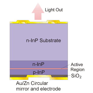
(a) Metalic Reflector VCSEL |
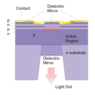
(b) Etched Well VCSEL |
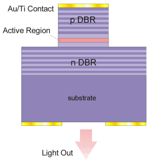
(c) Air Post VCSEL |
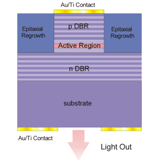
(d) Burried Regrowth VCSEL |
Cavity Issues
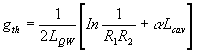
Today, most VCSEL devices employ quantum wells within the cavity. By depositing a thin layer of semiconductor with a slightly smaller band gap, one can not only define a region for recombination to occur, one can control over the optical properties of the device. Discrete energy levels are formed in the conduction and valence bands. Transitions from the conduction band to valence band energy levels occur from states that have the same value of n. Say, CC1-HH1 or CC1-LH1. The power obtained from a single quantum well is low. Multiple quantum wells may be grown within the cavity to increase power obtained. The position of the quantum wells is crucial if one is to maximise the gain of the device. Consider a standing wave in a cavity, with maximum amplitude 2P av at the anti-nodes and a spatially varying gain g(z), then the effective gain is given by:
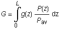
If we consider the case of a quantum well structure, where the gain medium is placed at a standing wave anti-node.
![]()
Distributed Bragg Reflectors (DBRs)
|
The reduced cavity length in VCSELs and the addition of quantum wells significantly reduces the probability of stimulated emission in a single pass of the cavity. The light within the cavity must be reflected back into the cavity many more times than with a Fabry Perot laser. The average time the photons spend within the cavity is known as the photon lifetime. The reflectivity of the mirrors must be very high to increase the photon lifetime and thus the time of interaction with the excited electron states. As an example, we obtain an estimate of the reflectivity that is required for these mirrors, we can apply some optimistic values to the gain threshold condition for a single quantum well device. Threshold gain occurs where the optical gain equals the optical loss. |

|
![]()
Expressed in terms of the gain:
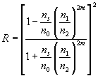
Where a is the absorption coefficient, L QW and L cav are the lengths of the gain region, and the quantum well respectively. R1 and R2 are the mirror reflectivities. Assuming an ideal device with no absorption. A final liberty will be to let R 1 = R 2 =R. Using a best case gain of 1000cm -1 give a mirror reflectivity of 99.95%. Metallic mirrors are limited to a reflectivity of ~98% and so for such small active regions are useless. Dielectric materials and semiconductors have a very low absorption coefficient for photons with energies below the bandgap energy of the material. If two dielectric materials, with a differing refractive index are placed together to form a junction, light will be reflected at the discontinuity. The amount of light reflected off one such boundary is small. However, if layers of alternating semiconductor or dielectric are stacked in a periodically, each layer with an optical thickness l /4n, the reflections from each of the boundaries will be added in phase to produce a large reflection coefficient. The number of layers required to produce a highly reflective mirror at a particular wavelength is determined by the difference in the refractive index of the contrasting materials. Also to be considered is the lattice constant of the materials, which must be matched within about one percent of the boundaries they are deposited, to avoid failure due to strain effects. Given the refractive index of the substrate n s and surrounding material (usually air) n 0 as well as the refractive indices of the contrasting semiconductors n 1 , n 2 for a given number of periods m the reflectivity is given by:
Mirrors for long-wavelength devices must be designed carefully, arranging a number of parameters. The most important considerations relate to the choice of materials used to fabricate the Bragg layers. These must be grown using materials that lattice-match to the material of the device cavity. The traditional choice of material for long wavelength devices has been GaAsInP/InP. However the contrast ratio between these two materials is very low. Therefore, a large number of alternating layers is required to achieve the high reflectivities demanded in VCSEL devices. Each layer of semiconductor increases the resistance of the device and raises the threshold current so it is important to minimise the number of layers required. Growing such Bragg reflectors puts considerable demands on the grower and makes for sporadic reliability. Highly reflective mirrors can also be fabricated from dielectric materials. Materials in common use are ZnSe/MgF and Si/SiO 2 .While dielectrics have a high refractive index contrast and can be deposited using low-temperature techniques they do not conduct an electric current. In addition, they are, in general, poor conductors of heat, an important consideration. Britney considers calculation of the reflectivity using transfer matrices here.
Current Confinement
As well as reducing the dimensions of the cavity one can reduce the threshold
current of a VCSEL device by limiting the cross-sectional area in which gain
occurs. There are a number of methods currently used in VCSELs.
A simple method is to etch a pillar down to the active layer. The large
difference in refractive index between the air and device material also act to
guide the light emitted. The problemw with this type of structure are the loss
of carriers due to surface recombination at the sidewalls and poor dissipation
of heat from the laser cavity.
Another technique for current confinement is ion implantation. By selectively
implanting ions into a semiconductor it can be turned into an insulating
material. Protons are most often used, however other ion species including F
+
, O
+
, N
+
and H
+
have been tried.
The bombarding of semiconductor with ions tends to damages the crystal
structure of the implanted material and so it must be used with caution within
close proximity to the active layer.
The formation of an insulating apeture of aluminium oxide between the cavity
layer and the one of the Bragg reflectors . This starts as a layer of AlGaAs.
In a steam environment of 350deg C to 500deg C the AlGaAs is converted into an
oxide layer. The rate of formation of the oxide layer is proportional to the
content of Al in the material; thus the oxide forms first in those layers with
the highest aluminium content. The oxide layer has a low refractive index
compared with the semiconductor and thus also acts as a waveguide for the
emitted light. Much research has concentrated on lateral oxidation for use with
near infrared devices; A 1.5
m
m cw VCSEL was announced by Their device consisted of a InGaAsP-InP active
region and mirrors of AlGaAs/GaAs and GaAs/AlAs bonded by wafer fusion.
Optical Power and Differential Quantum Efficiency
The optical output power is
![]()
where h depends on two factors: (1) the injection current efficiency accounting for the fraction of injected carriers contributing to the emission process (some the carriers can recombine in the undoped confinement regions where the carriers do not interact with the optical field), and the (2) the optical efficiency accounting for the fraction of generated photons that are transmitted out of the cavity. Note that the threshold current depends on the injection current as well as on the junction temperature T jct . The differential quantum efficiency is then current dependent:
![]()
We see that h (I) ext can be negative if di th /di>1. The light output P out vs. the injection current will have a negative slope.
References
[1] I. Melngailis,
Longitudinal injection-plasma laser of InSb
,
Applied Physics Letters
,
6
, No.3, pp 59-60. (1965)
[2] R. Potter,
Surface Emitting Lasers
,
1998 MPhil Dissertation, University of Essex
[3] R. D. Burnham, D. R. Scifres, and W. Striefer,
Single-heterostructure distributed feedback GaAs diode lasers
,
IEEE J. Quant. Elec.
QE-11
pp 439-449 (1975)
[4] Zh. I. Alferov, V. M. Andreyev, S. A. Gurevich, R. F. Kararinov, V. R.
Larionov, M. N. Mizerov, and E. L. Portnoy,
Semiconductor lasers with the light output through the diffraction grating on
the Surface of the waveguide layer
,
QE-11
pp 449-451 (1975)
[5] H. Soda, K. Iga, C. Kitahara and Y. Suematsu,
GaInAsP/InP Surface Emitting Injection Lasers
,
Jpn. J. Appl. Phys.
18
, pp 2329-2330 (1979)
[6] A. Chailertvanitkul, S. Uchiyama, Y. Kotaki, Y. Kokobun and K. Iga,
Annual Meet. Jpn. Soc. Appl. Phys. Tokyo, Japan
(1983)
[7] I. Ibaraki, S. Ishikawa, S. Ohkouchi and K. Iga,
Elec. Letts.
20
pp 420 (1984).
[8] D. L. Huffaker et al.
Sub-40mA continuous-wave lasing in an oxidized vertical cavity surface-emitting
laser with dielectric mirrors
,
IEEE Photon. Tech. Lett.
8
, pp 974-76 (1996).
|
|