|
|
PIN diode Structures
J.Y. Wah, C. J. Hepburn
Overview
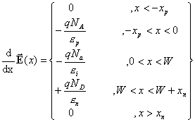
A p-i-n diode is a p-n junction with a doping profile tailored so that an intrinsic layer, the 'i region,' is sandwiched between a p layer and an n layer. In practice, however, an idealized i region is approximated by either a high-resistivity p layer (referred to as p layer) or a high-resistivity n layer ( n layer). The nature of the low doping in the i region, causes most of the potential will drop across this region. To model this diode structure,we must first define the space charge distribution and then work out the electric field in each region. Applying continuity of displacement vector at each of the boundaries, the electric field can be deduced. The electrostatic potential profile is then obtained by integrating the electric field. Let us start by defining the space charge distribution of PIN diode.
(1)
From Gauss's law
![]()
(2)
Integrating equation (2) and we obtain
(3)
Boundary condition gives
(4)
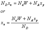
Electric field is the negative gradient of electrostatic potential, therefore from equation (3) and using the fact that electrostatic potential continuous at each boundary. We obtain,
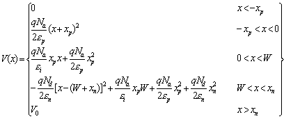
(5)
where
![]()
(6)
P- p -N and P - n -N depletion length x p Calculation
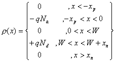
We are now interested in modelling the P- p -N or even P- n - N. The space charge distribution is:
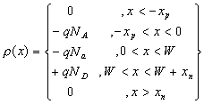
(7)
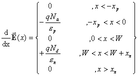
where N A , N a , and N D are the dopant concentration in P, p , and N region respectively. Then Gauss's law gives
(8)
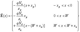
The corresponding electric field is
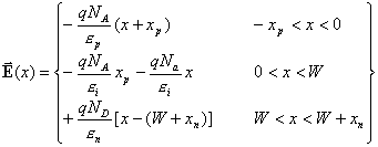
(9)
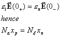
Boundary conditions at W
![]()
and hence
(10)
The electrostatic potential is
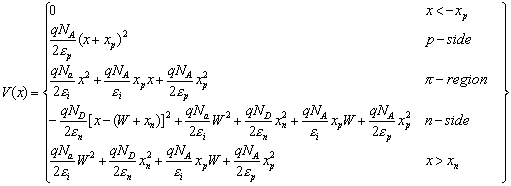
(11)
The built in voltage is defined as
![]()
(12)
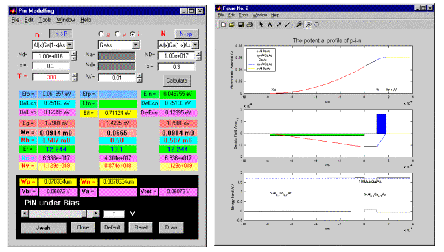
PIN Modelling

|
|
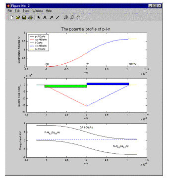
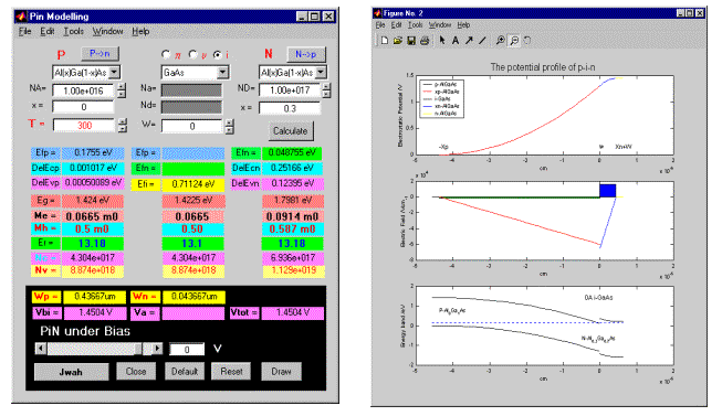
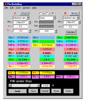
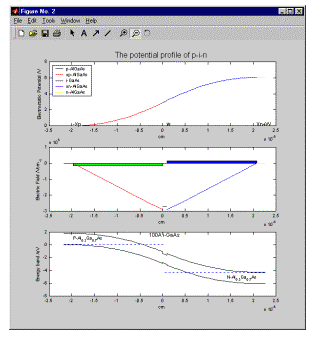
Figure 1. This is the PIN Homojunction with W=0 m m, Al x Ga (1-x) As, x=0.3 on each side, N A =N D =1x10 17 cm -3 , and temperature T=300 K. With the same material on both sides the electric field is continuous at the junction. W p =0.10 m m, W n =0.10 m m, V bi =1.627 V
Heavily doped in p and n region
Isotype n-N Heterojunction Modelling
Anisotype p-N Heterojunction Modelling
Anisotype P-n Heterojunction Modelling
PIN under forward bias

|
|
PiN under reverse bias
|
|
Approaching a Quantum Well
|
|
|
|