|
|
Semiconductor Junctions: n-P Heterojunction
Written by J. Y. Wah, C. J. Hepburn.
If the narrow band gap semiconductor is doped n-type and the larger gap semiconductor is doped P-type. When they are brought together, a space charge will exist due to the diffusion and redistribution of free carriers at thermal equilibrium.
The space charge distribution r (x) is
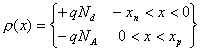
(1)
The electric field is proportional to integal of the charge distribution, Therefore the field will be
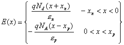
(2)
where the boundary condition at x = 0 gives
![]()
(3)
The electrostatic potential is
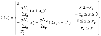
(4)
where
![]()
(5)
Therefore with equations 3, 4 and 5 the depletion length of x p is as
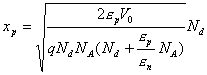
(6)
The energy band edges function E c (x) and E v (x) can be obtained from qV(x)
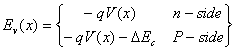
(7)
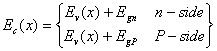
(8)
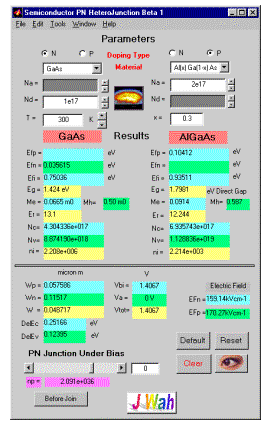
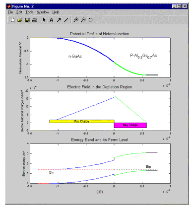
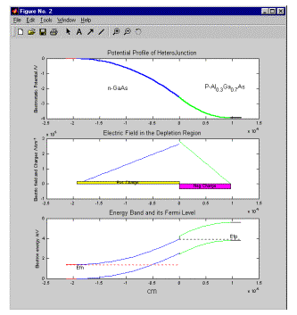
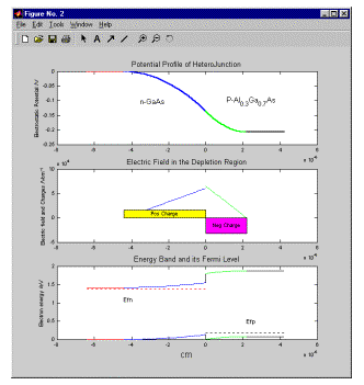
nP HeteroJunction Modelling
Using the software, we show the potential, electric, field, and energy band profiles for a n-GaAs, P AlGaAs heterojunction under equilibrium conditions of zero bias and then under reversed and forward bias respectively.
|
Figure 1: nP heterojunction Modelling at thermal equilibrium, i.e. V a = 0. The two figures on the bottom, on the left is the junction under reverse bias, on the right is forward bias.
|
|
|
|