|
|
High-Field Effects
|
|
|

Drift-velocity with Increasing Electric Field
The semiconductor drift-velocity is linear with the electric-field if the drift-velocity is small compared to the thermal velocity. In this regime, it is restatement of Ohm's law.
![]() for
electrons
for
electrons
(1)
![]() for
holes.
for
holes.
(2)
As the electric-field is increased, the drift-velocity departs from this linear relationship. The drift-velocity starts to decrease and eventually saturates. For semiconductors that show saturation. It can be approximated by
![]()
(3)
where E is the electric-field, m is the mobility and v sat is the saturation velocity.
|
Material |
v sat x10 7 v |
m |
|
Si |
1 |
1400(e), 450(h) |
|
Ge |
1 |
3900 (e),1900 (h) |
|
InP |
0.67 |
- |
|
GaN |
2.5 [2] |
- |
|
AlAs |
0.85(n) ,0.8(p) [4] |
- |
|
InN |
2.5 |
-
|
Table 1. Values of parameters used in (3) for some common semiconductor materials.
Using this data, the drift-velocity of carriers against electric field is shown below:
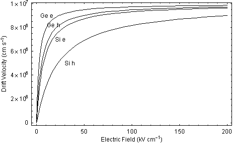
Figure 1. Drift-velocity against electric-field for electrons and holes in Silicon at T=300 K.
Saturation occurs because as the electric field heats the carriers giving them more energy. Higher energy carriers scatter more strongly and so the drift-velocity reaches a constant value.
Hot-Electrons
Hot-electrons occur when a strong electric field is applied across a semiconductor. The electrons obtain energy from the applied electric field, which they dissipate by emitting phonons, exciting other electrons or emitting photons. When an electron's energy exceeds the average thermal energy of the semiconductor, the increase in kinetic energy of the electrons is statistically interpreted as a raising of the electrons' temperature, so they are termed 'hot electrons' . A rough estimate of the threshold electric-field, E th required to create hot-electrons is given by Ridley [1]

(4)
Where E 0 is the energy with zero applied field, and m and t E are the mobility and the energy relaxation time measured at zero field. Typically, E th is about 1kV cm -1 .
Negative Differential Resistance (NDR)
With GaAs and InP, the high-field behaviour of the drift-velocity does not follow this pattern of saturation but actually the drift-velocity reaches a peak and then starts to decrease. This is because the band structure in these materials has more than one local minima in the conduction band. Figure 2. shows a simplified conduction band diagram for GaAs. The lowest conduction band minima is at the G point ( k =0). At this point the electrons have a low effective mass and a high mobility. A second local minimum occurs at the edge the Brillouin zone and is 0.36 eV higher. This minimum has a higher effective mass and therefore a lower mobility (see Mobility (3)). At low electric-fields, nearly all of the conduction electrons will occupy the lower minimum at k =0 with the lesser effective mass and high mobility. If the electric-field increased gradually to about 3.2 kV cm -1 , the electrons will have enough energy to occupy energies in the second minima with its associated higher effective mass and lower mobility. As the field is increased further, the proportion of electrons with the lower mobility increases and the drift-velocity will continue to decrease until all the electrons share the lower mobility and the drift-velocity will level off. This drop in velocity with increasing field was suggested by Ridley and Watkins in 1961 and discovered in 1963 by Gunn, after whom the effect was named.
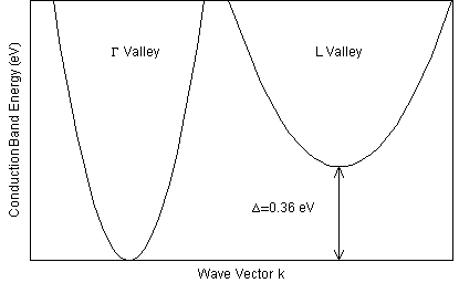
Figure 2. Simplified band structure of GaAs. When the electrons acquire at least 0.36 eV they have enough energy to transfer to the satellite valley. This transfer of electrons is the cause of negative differential resistance (NDR).
Transferred Electron Devices (Gunn Diodes)
The Gunn diode is formed by adding metal contacts at the ends of a doped semiconductor material, which shows negative differential resistance (usually GaAs) as shown in Figure 3 (a). When biased in the negative differential resistance region, random perturbations in the net charge as a result of thermal motion of electrons cause the formation of charge domains which travel with the electric-field until they are absorbed at the anode of the device. Figure 3 explains the formation and growth of these Gunn domains. Initially, the device is biased at E 0 , which is within the negative differential resistance regime. A local perturbation in the net charge density causes a build up of negative charge (A) with an associated region to the right of the perturbation where there are fewer charge carriers (B) as indicated in Figure 3 (b). From the electric-field - drift-velocity characteristic, Figure 3 (c), it is clear that in the negative differential resistance regime, the drift-velocity is higher for regions E A and lower at E B . Therefore, the electrons pile up as they travel with the electric-field and the domain grows as shown by C and D in Figure 3(b). The domain will continue to grow until the drift-velocity of the electrons is the same. This occurs at v c for E C and E D .
With drift-velocities of the order of 10 7 cm s -1 and device length of a few microns, the frequency of theses devices is of the order of 10 10 Hz or tens of Gigahertz, which is in the microwave frequency. In practice, with this simple device, the frequency of operation is limited by a 'dead-zone' near the cathode in which no Gunn domains form. Thus the device length is constrained by the incorporation of the dead zone. More advanced designs include heterostructures or a notched doping profile to decrease the length of the dead zone.
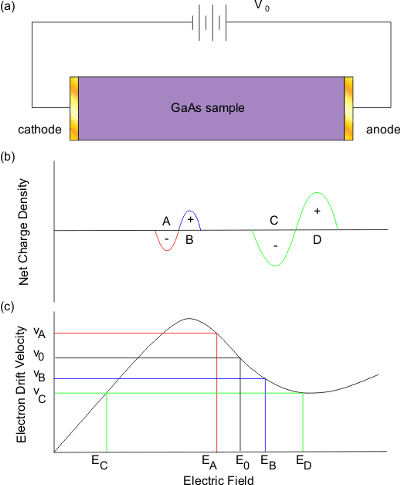
Figure 3. (a) Gunn diode structure. (b) Net Charge density in a Gunn Domain. (c) Electric-field drift-velocity characteristics.
Avalanche Breakdown
Eventually the electric-field becomes so great that the semiconductor material breaks down. The electrons hole pairs acquire enough energy to ionise atoms in the lattice and the electric-field accelerates these electrons and holes to ionise more atoms in a process known as impact ionisation . In this way, a few electrons can lead to a runaway chain reaction which cause a breakdown in the material. This is known as avalanche breakdown. The critical voltage at which breakdown occurs V br is given by
![]()
(5)
Where E br is the electric-field at which breakdown occurs, e s is the relative permitivity, q is the electron charge in eV and N d the doping density. At T=300 K, the breakdown field are given below for various common semiconductors.
| Semiconductor | Breakdown Field; |
|---|---|
Table 1. Electron and Hole mobilities for various semiconductor materials
Table 2. Critical Electric-fields in kV cm -1 for common semiconductor materials at T=300 K.
Using (5) we plot the breakdown voltage against doping density.
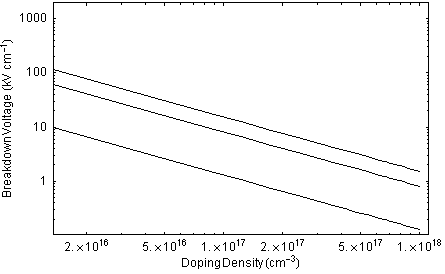
Figure 4. Breakdown voltage against doping density at T=300 K.
References
[1] N. Balkan, "Hot Electrons"
[2] Michael S. Shur and M. Asif Khan, Mat. Res. Bull. 22 (2), 44 (1997).
[3] U. V. Bhapkar and M. S. Shur, J. Appl. Phys., 82 (4), 1649 (1997).
[4] Pozhela, J. and A. Reklaitis, Solid State Electron. 23 , 9 (1980) 927-933.
[5] R. Quay, C. Moglestue, V. Palankovski, and S. Selberherr, Mater. Sci. Semicond. Process. , 3 , 1-2, (2000), 149-155.
|
|
|
|