|
|
|
|
Semiconductor Crystals
The Lattice and the Basis
A crystal is a regular, ordered arrangement of atoms over a large scale. The atoms may be of a single type or the repetition of a complex arrangement of many different types of atoms. The crystal can be thought of as consisting of two separate parts: the lattice and the basis. The lattice is an ordered arrangement of points in space, while the basis consists of the simplest arrangement of atoms which is repeated at every point in the lattice to build up the crystal structure. A good analogy is patterned wallpaper. The basis is like a motif on the wallpaper and the lattice would be periodic pattern of points on which of the motif is repeated. In Figure 1, the lattice points correspond with the centre of the basis, but this does not have to be the case.
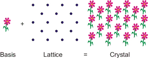
Figure 1. A crystal can be thought of as being like wallpaper. The motif is analogous to the basis and the arrangement of the motif over the surface is like the lattice.
The points on the lattice are specified using vectors. Lattice vectors are the shortest distances to the nearest neighbouring points on the lattice and are conventionally denoted by a, band c. The angles between these vectors are given the symbols , α, β and γ. A simple two-dimensional example is shown in Figure. 2. Any two lattice points can be reached using a combination of the lattice vectors a and b. Obviously, in three dimensions, any point on the lattice can be reached using a combination of the three lattice vectors a, b and c. In 2-dimensions this is,
![]()
The basis vector , R is a vector from one lattice point to another in terms of the lattice vectors. Since the lattice looks the same (invariant) in going from one lattice point to another, the lattice has translational symmetry.
Primitive Cell
The primitive cell is the smallest part of the lattice that if repeated would reconstruct the entire crystal structure.
The unit cell - is a volume repeated throughout the entire lattice. The unit cell does not have to be the primitive cell.
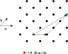
Figure 2. Lattice vectors are a linear combination of the basis vectors.
The Fourteen Bravais Lattices
The ways in which we can specify the lattice points in space and keep translational symmetry is limited. In 1848, Auguste Bravais demonstrated that there are in fact only fourteen possible point lattices and no more. For his efforts, the term Bravais lattice is often used in place of point lattice.
|
System |
Number of Lattices |
Lattice Symbol |
Restriction on crystal cell angle |
|
Cubic |
3 |
P or sc, I or bcc,F or fcc |
a=b=c |
|
Tetragonal |
2 |
P, I |
a=b≠c |
|
Orthorhombic |
4 |
P, C, I, F |
a≠b≠ c |
|
Monoclinic |
2 |
F, C |
a≠b≠ c |
|
Triclinic |
1 |
P |
a≠b≠ c |
|
Trigonal |
1 |
R |
a=b=c |
|
Hexagonal |
1 |
P |
a=b≠c |
Table 1. Seven crystal systems make up fourteen Bravais lattice types in three dimensions.
P - Primitive: simple unit cell
F - Face-centred: additional point in the centre of each face
I - Body-centred: additional point in the centre of the cell
C - Centred: additional point in the centre of each end
R - Rhombohedral: Hexagonal class only
Miller Indices and Notation
Miller Indices are used to identify planes of atoms within a crystal structure. Miller indices are written as three digits between brackets, (100) for example. Given the intercepts of the plane with the crystallographic axes. (directions of the lattice vectors), joining the intercepts with lines defines a plane which cuts through the crystal. The Miller indices are calculated by taking the reciprocal of the intercepts and multiplying them by their highest common factor. Negative numbers are represented by placing a bar over the top of the digit. If this sounds at all complicated, it is easily illustrated with a few examples. If the intercept is at infinity, then the plane is parallel to that axis and the Miller index is zero, since, 1/&inf; =0.
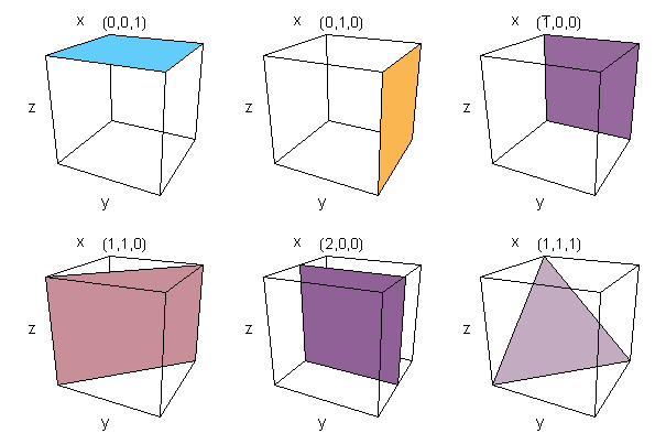
Figure 3. Example Miller indices showing the plane of atoms they represent
The diligent reader may have noticed that due to the symmetry of the unit-cell of the lattice, certain planes are equivalent. In the cubic lattice, for example, (100) is equivalent to five other planes, (010), (001), (100), (010), (001) and to acknowledge this, the set of Miller indices is written {100} which means the set of (100) planes equivalent by virtue of symmetry. The beauty of this system is that similar planes can be identified in any of the Bravais lattice point groups. The Miller indices are also similar in the way in which planes are described in mathematical terms.
As we saw earlier, a vector from one lattice point to another can be specified in terms of the lattice vectors of the primitive cell. A common shorthand notation to show the lattice vector directions is to write the three vector components coefficents in square brackets [uvw ] where u, v, and w are integers, although it is important not to confuse these with Miller indices. The direction is then
![]()
(1)
Equivalent directions are designated using angled brackets <uvw >.
The Reciprocal Lattice
The reciprocal lattice is the collection of points that represent allowed values of wavevectors for Fourier series and Fourier transforms with the periodicity of the lattice. The value of k allowed for any vector is given by
![]()
(2)
where f(k) is the Fourier transform of f(r). The value of k for a second point (also on the lattice) f(r+R) is
![]()
(3)
Since the lattice is periodic, we would expect that any 2 points on the real-space lattice would return the same value of k. Therefore, equations (2) and (3) become equal if
![]()
(4)
This restriction allows only certain vectors {k}. Vectors that satisfy (4) are given by
![]()
(5)
Finally, the vector k is more conventionally given the symbol G.
![]()
(6)
Where h,j,l are integers and the vectors a * , b * and c * are the reciprocal lattice vectors. In terms of the lattice vectors a , b , c the reciprocal lattice vectors a * , b * and c * are given by:
![]()
(7)
The denominators in (6) are the volume of the unit cell and so act as a normalisation constant. Using the relations for the lattice and the reciprocal lattice the transformation from real lattice to reciprocal lattice can be calculated.
Wigner-Seitz Cell
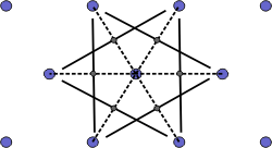
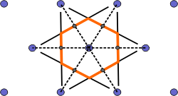
The Wigner-Seitz cell is a primitive cell which displays the full symmetry of the lattice. The Figure below shows the construction of a Wigner-Seitz cell. In reciprocal space, the Wigner-Seitz cell is also a Brillouin zone and we shall use it to construct Brillouin zones later.
|
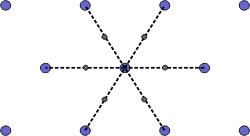
a) Select a lattice point and draw construction lines to the nearest neighbouring points. |
|
b) Draw lines that perpendicularly bisect the construction lines |
|
c) The smallest enclosed area represents the Wigner-Seitz cell. Here shown in orange. |
Figure 4. Construction of the Wigner-Seitz cell.
Brillouin Zones
The Brillouin zone is defined in the reciprocal lattice as the volume enclosed within a Wigner-Seitz cell. At the boundaries of the Brillouin zone, the Bragg diffraction condition in the reciprocal lattice must be satisfied.
![]()
(8)
Where k' is the wavevector of the diffracted wave and k is the incident wavevector and G is a reciprocal lattice vector. Squaring (8) gives,
![]()
(9)
and assuming the wave is elastically scattered, then k' 2 = k 2 . Equation (9) becomes 2 k × G =- G 2 . Finally, if G is a lattice vector then so is - G and the equation can be rewritten as
![]()
(10)
The geometric interpretation of equation (10) is that the diffraction condition is satisfied if k lies in the plane that perpendicularly bisects the lattice vector G.
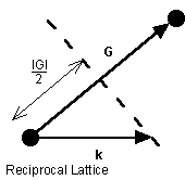
Figure 5. The geometric interpretation of the Bragg diffraction condition that gives rise to Brillouin zone boundaries.
In order to construct the Brillouin zones (BZ), we use the construction method for the Wigner-Seitz cell (WS) outlined above but using the reciprocal lattice space. Further Brillouin zones can be constructed by taking the next nearest set of lattice points from the starting point and repeating the process.
Since the lattice and reciprocal lattice are related, the WS cell defined in real space and the WS in k-space are also related. In particular, the WS defined in the bcc real space lattice gives a fcc BZ in reciprocal lattice and vice versa.
|
Lattice Real Space
|
Lattice k-space
|
|
bcc WS cell |
fcc BZ |
|
fcc WS cell |
bcc BZ |
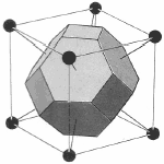
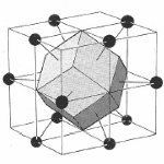
Figure 6. The transformation of the WS cell of bcc lattice in real space transforms to a Brillouin zone in a fcc lattice in reciprocal space while the WS cell of a fcc lattice transform to a Brillouin zone of a bcc lattice in reciprocal space.
Points of symmetry on the Brillouin zone are given particular importance especially when determining the bandstructure of the material.
Electrons in the semiconductor are perturbed by the potential of the crystal. The bandstructure of the semiconductor are the allowed energies that the electrons can have. These bands of energy vary with k-space (reciprocal lattice space). Therefore, points of high-symmetry on the Brillouin zone have specific importance. Perhaps the most important, at least for optoelectronic devices, is at k = 0 which is known as the gamma point. As you might expect, it is given the symbol, Γ .
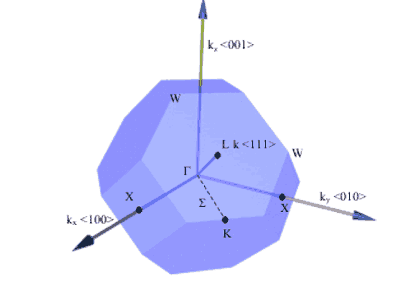
Figure 7. Some important symmetry points on the Brillouin zone of a fcc crystal (real space) and directions of planes. [1]
|
Symmetry Point
|
k
|
|
Γ
|
kx= 0, ky= 0, kz= 0
|
|
X
|
{ki= ±2π /a, kj= 0, kk= 0}
|
|
L
|
{kx= ±π/a, ky= ±π/a, kz= ±π/a}
|
Table 2. k-vectors of the important symmetry points for the fcc crystal structure. The indices for X points are a cyclic permutation of axes. E.g. If i=x then j=y, k=z. If i=y then j=z and k=x,etc.
Crystal Structures of Semiconductors
By far the most common crystal structure in semiconductors is the zincblende structure, sometimes known as sphalerite. Closely related to the zincblend structure is the diamond crystal structure. The only difference between the zincblende and diamond structures, is that in the diamond formation there is only one type of atom in the crystal. Real Diamonds also have the diamond crystal structure.
Some semiconductors can have more than one type of crystal structure depending on the conditions in which they are grown. The Nitride semiconductors for example, GaN, InN and AlN can crystallise in either the Wurtzite or Zincblende structures.

Figure 8. Diamonds might be a girl's best friend, but their crystalline structure is closely related to the zincblende structure.
The zincblende structure is described by two interpenetrating face-centred cubic lattices. One type of atom is located on one of the face-centre cubic lattices and the second type of atom is located on another face-centre cubic lattice which is displaced by 1/4( a , a , a ) as can be seen in the 3d model in Figure 8 where the two lattices are coloured orange and blue to distinguish them.
Figure 8. 3D model of Zincblende structure.
The Wurtzite structure can be thought of as two interpenetrating hexagonal close packed lattices.
Figure 9. 3D model of Wurtzite GaN structure.
References
[1] J. Y. Wah, PhD Thesis, University of Essex, (2003).
|
|