Intrinsic and Extrinsic Semiconductors

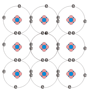
A semiconductor is said to be intrinsic if it only contains those atoms make up the crystal structure. At absolute zero, the valence band is completely filled. Conduction takes place as electrons gain enough thermal energy to overcome the energy gap. As temperature increases, the thermal energy of the valence electrons increases allowing more of them to breach the energy gap into the conduction band. Thus, unlike metals, in semiconductors, the resistance decreases with temperature. When an electron gains enough energy to escape the electrostatic attraction of the atom, it leaves behind a vacancy which may be filled be another electron. The vacancy produced can be thought of as if it were a carrier of positive charge.These vacancies in the valence band are known as a holes. As electrons flow through the semiconductor, holes flow in the opposite direction. If there are n free electrons in an intrinsic semiconductor, then there must also be n holes. Holes and electrons created in this way are known as intrinsic charge carriers. The carrier concentration or charge density defines the number of charge carriers per unit volume. This relationship can be expressed as n=p where n is the number of electrons and p the number of holes per unit volume. The variation in the energy gap between different semiconductor materials means that the intrinsic carrier concentration at a given temperature also varies.
|
fig. 1. Intrinsic semiconductor material |
Extrinsic Semiconductors
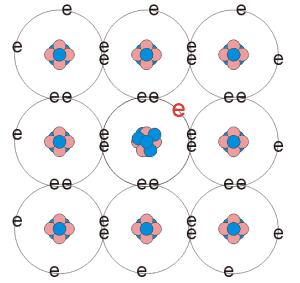
Doping the material with impurity atoms is a way of changing the number of charge carriers in the material. By adding a small fraction of an atoms (about 1 in a million) the number of carriers can be changed altering the conducting properties of the crystal. For example, suppose that we start with Silicon, which has a valance of four. That is, it has four electrons in it outer most shell. The atoms will arrange in such a manner as to reduce the energy required to bond together. The sharing the electrons with neighboring atoms, as covalent bonds, each atom can form a stable outer shell of electrons. If atoms with a valance of five, As (Arsenic), for example, is added at the time of growth, then an impurity atom can replace one of the Silicon atoms. Four of its five bonds will become covalently bonded to its neighbouring Si atoms. The fifth electron is weakly bound to the As nucleus and thus very little energy is required to ionise the atom. The electron can then participate in the conduction process. By adding atoms of even greater valence than the atoms in host material, these impurities can be used to donate more than one electron per impurity atom replaced at a lattice site. The impurity atom is said to be a donor because it gives up its weakly bound electrons leaving a positively charged nucleus. Material doped in this way is often referred to as n-type semiconductors because the majority carriers are electrons.
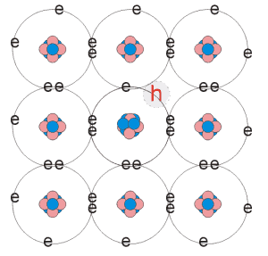
Introducing atoms with a valance one less than that of the atoms in the host material, such as B (Boron), there are not enough bonds to form a stable outer shell of electrons. The nucleus, however is of a similar potential to the Silicon atoms. To create a stable shell, the Boron atom has to capture an electron from a neighbouring atom, this causes the vacancy to propagate. The nucleaus of the Boron atom has a similar electrostatic potential to the Silicon atoms therefore it is possible for an electron to pulled from a neighbouring Silicon atom. The capture of an electron from another atom results in the vacancy being propagated further along the crystal. This propagation can be thought of as the flow of positive charge since the vacancies move in the opposite direction to that of the electrons. The absence of electrons is known as a holes and dopant atoms that cause that create the holes are known as acceptor impurities since they accept charge. Semiconductor material doped in this way is known as p-type. The diagram below summaries the above discussion.
|
fig. 2.a) n-type doped semiconductor |
b) p-type doped semiconductor |
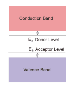
The effect of the dopant impurities in a semiconductor is to alter the bandstructure of the material. If we plot energy as a function of position, n-type dopants alter the local bandstructure giving rise to energy levels within the energy gap just below the conduction band minimum. While p-type dopants create local energy levels within the band-gap just above the top of the valence band. This is illustrated in the fig. 3.
|
fig. 3. donor and acceptor impurity atoms added to intrinsic semiconductor have the effect of locally reducing the band gap of the semiconductor, increasing the conductivity of the material. |
 |